
DSFP MSA is mainly for DSFP interface, optical module electrical performance interface and mechanical specification, so DSFP design is mainly hardware design.
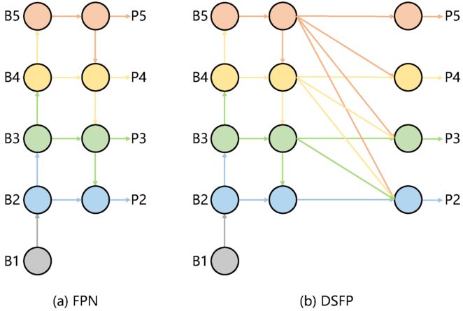
DSFP provides a dual-lane PAM4 high-speed Serdes interface, and the DSFP optical module can be directly connected to the Switch ASIC through a two-receive and two-transmit high-speed channel.
For the connection between TD2 and RD2 pairs of high-speed Serdes and DSFP optical modules, if SFP+/SFP28 optical modules can be connected, a 0.1 μF AC coupling capacitor needs to be connected in series to protect the high-speed Serdes interface RD2+/- and TD2+/- of the ASIC. be damaged. At the same time, the DSFP MSA also recommends that the ASIC first turn off TD2+/-, and then turn on TD2+/- after detecting that the access is a legal DSFP module. The IIC management interface can be managed by FPGA or CPU. The most important thing is the design of a bidirectional dual-function circuit. The following mainly introduces the circuit connection of LPWn/PRSn and INT/RSTn pins.
According to the design of the three-voltage area, the single-board circuit needs to provide a 2.5 V reference power supply, which can be obtained through the DC/DC power conversion chip. The 1.25 V reference power supply is used by the DSFP optical module and will be integrated in the optical module. For the design of the switch, only the design of the host side should be considered, that is, the design of the 2.5 V reference power supply can be considered. As shown in Figure 3, for a bidirectional design circuit using a voltage comparator, use a dual op amp LM393, and the dual op amps are applied to LPWn/PRSn and INT/RSTn respectively, so each interface needs an LM393.
The LPWn/PRSn signal of DSFP is connected to the positive terminal of the comparator. When DSFP is not in position, the voltage of PRSn is 3.3 V due to the pull-up 10 kΩ resistor, and the positive terminal voltage of the comparator is greater than the negative terminal voltage of 2.5 V. The comparator Output a high level to the FPGA, indicating that the module is not in place; if the DSFP is in place, because the DSFP has a pull-down 10 kΩ resistor inside, due to the voltage division of the pull-down resistor, the positive terminal voltage of the comparator is 1.65 V, which is less than the negative terminal voltage 2.5 V, the comparator outputs a low level to the FPGA, indicating that the DSFP module is in place. In the SFF-8431 specification, the presence signal Mod_ABS of the SFP+/SFP28 optical module is directly grounded inside the module, which is also one of the differences between DSFP and SFP+/SFP28.
The FPGA is connected to the positive side of the voltage comparator through an I/O pin (configured as an output). When it is necessary to control LPmode, the FPGA output is Low, which will directly make the DSFP pin receive 0 level, and set it to Low power mode; otherwise, if it needs to be set to High power mode, the FPGA output pin is high impedance, at this time The pin level of LPWn is about 1.65 V due to voltage division by pull-up and pull-down 10 kΩ resistors, which is higher than the 1.25 V judgment value in the DSFP module, so the module is set to High power mode.
The INT/RSTn signal of the DSFP is connected to another voltage comparator of the LM393, which pulls down a 68 kΩ resistor to GND. When the DSFP is in position, the pin has a 5 kΩ resistor to pull up the voltage to 3.3 V. When the DSFP has an interrupt, the DSFP module will turn off its internal 8 kΩ pull-down resistor, so that the level of the INT/RSTn pin is pulled up by the internal 5 kΩ and external pull-down 68 kΩ, which is greater than the 2.5 V reference voltage, causing the output of the voltage comparator to be 0, and notifying the FPGA of an interrupt; otherwise, when there is no interrupt, the DSFP module will turn on its internal 8 kΩ pull-down resistor, so that INT/ The level of the RSTn pin is determined by the internal pull-up 5 kΩ, pull-down 8 kΩ and external pull-down 68 kΩ, the voltage is about 1.9 V, if it is lower than 2.5 V, the voltage comparison output is high, and FPGA reception is not interrupted.
The above circuit design has been modified on the basis of referring to the DSFP MSA specification. With the help of the FPGA function, the design connection is simpler and the control is more convenient.
DSFP control method
In the power supply circuit of the DSFP optical module, the power switch is used for current limiting protection of its power supply to prevent the 3.3 V power supply circuit of the DSFP from overcurrent or even the inductance being burned due to problems such as wrong insertion of the optical module or short circuit due to damage to the optical module. Condition. The current limit value can be determined according to the power level of the DSFP optical module used. The specific DSFP module control method is suggested as follows:
After power-on, the FPGA will turn off the power switches of each DSFP by default, and at the same time set the LPmode output pin to low level, and enable it to Low Power mode by default, and reset the pin output to low level by default. When the FPGA detects that the DSFP optical module is in place, turn on the power switch, but keep the reset and Lower power, then release the Reset after a delay of 10 ms, and release the Lower power mode to High power mode after another 10 ms. If it is detected that the DSFP module is not in place, turn off the power switch at the same time, enable reset and enable Low power mode.
Other usage specifications
The SMT connector of DSFP is not compatible with SFP+/SFP28, but its Cage is compatible with SFP+/SFP28, which makes the mechanism design consistent with SFP28. The use of BOM needs to pay attention to the power consumption level of DSFP, so as to decide whether to update the heat sink on the basis of SFP28. In some applications with low power consumption, the cage of SFP28 can meet the requirements of DSFP.
The SMT connector of DSFP is not compatible with SFP+/SFP28, but its Cage is compatible with SFP+/SFP28 (click here), which makes the mechanism design consistent with SFP28. The use of BOM needs to pay attention to the power consumption level of DSFP, so as to decide whether to update the heat sink on the basis of SFP28. In some applications with low power consumption, the cage of SFP28 can meet the requirements of DSFP.